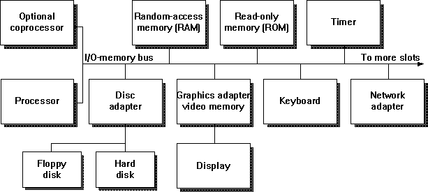
To get a handle on the bottleneck issue, we need to understand just a little about how our computer is organized internally. Figure 2.1 is a block diagram of the hardware organization of the original IBM® personal computer. Modern systems may partition things a bit differently, but the basic idea has not changed much since the early 1980's.

Figure 2.1 Block diagram of the original IBM personal computer
Actually, Windows NT will not execute on one of the original PCs, because those PCs used a processor that's just too punya 16-bit processor, instead of a 32-bit processor. A more modern system, based on the Intel® 486 chip, is shown in Figures 2.2 and 2.3.

Figure 2.2 Block diagram of a current Intel 486-based computer
Just as some perfectly competent auto drivers don't know how spark plugs work, some perfectly competent computer users might not know how programs execute on the architectures represented by the illustrations in this section. Programs are composed of instructions that reside initially on the disk drive or across the network on some other computer's disk drive. The processor executes these instructions and follows their logic. It is typical for Intel 486 processors to take about 2.75 processor cycles per instruction, on average. The processor is running at a cycle rate determined by the system clock. Typical cycle rates today vary from 25 MHz to 100 MHz, (megahertz, or millions of cycles per second). A 66-MHz 486 executing at a rate of, say, 2.75 cycles per instruction will observe an instruction rate of approximately
(66,000,000 cycles/sec) / (2.75 cycles/instruction)
or 24,000,000 instructions per second.
In RISC architectures, the design goal is to execute one or two instructions in every clock cycle. The price for this speed is a simpler instruction set, and hence a compiler needs to generate about 20% more instructions to do a given job. Achieving this design goal is also heavily dependent on the effectiveness of the cache hierarchy, and RISC systems tend to benefit from large caches. Because caches are cheaper than processor chips, this is a reasonable approach.
When told to execute a program, Windows NT must bring the program into RAM. Windows NT does this in pages so the whole program does not have to be in memory at one time. This is called demand paging. Why use paging at all? To efficiently use a scarce resourceRAM.
Control is transferred to the instructions in the program. Instructions are brought from RAM into the processor and tell the processor what to do next. The program can ask Windows NT to read file data from or write file data to the disks or the network. This causes the data to pass from RAM to the adapter, which takes care of transferring data to or from the media. On completion of the operation, the adapter interrupts the processor.
The program can ask Windows NT to draw text or graphical images on the display using the graphics adapter. In this case, the bits flow from RAM memory to the video memory on the graphics adapter, or else the image is drawn directly into video memory. Whatever is in video memory is automatically displayed on the monitor by the graphics adapter hardware. The program can also ask Windows NT to notify it when you press a key on the keyboard or move the mouse, which can also be attached to the I/O-memory bus.
You may have guessed by now that all this movement of data is on the I/O-memory bus. This is not a wheeled vehicle inside your machine that ferries data around, but there is absolutely nothing wrong with thinking of it as one. The bus is really a collection of printed circuit board traces along which electrons scream at about half the speed of light. Unfortunately, the circuitry controlling the bus access and routing slows things down quite a bit. In the design in Figure 2.1, the processor and the I/O-memory bus run at the same rate: 8 MHz. One big difference between Figures 2.1 and 2.2 is the partitioning of the system hardware into two separate buses, so slower I/O traffic does not interfere with the high-speed processor memory traffic of today's systems. These buses are fast enough that they are seldom a computer system bottleneck. There are exceptions, however, and we'll mention a few later on.

Figure 2.3 Memory bus organization of a current Intel 486-based computer
The two memory caches detailed in Figure 2.3 help form a memory hierarchy, which speeds system operation considerably while also reducing bus traffic. The cache built into the 486 processor is 8K and holds recently used code and data. This exploits a well-known property of programsa program uses many of the memory bytes that it has used in the recent past. This is called locality. By keeping these bytes near the processor in high-speed (expensive) memory, access to them is much more rapid. Usually it takes one processor cycle to fetch something from the first-level cache. The second-level cache is larger, slightly cheaper memory that is not in the processor chip itself. The second-level cache can usually be accessed in two processor cycles. It is not unusual for a main memory access to take around 10 processor cycles, so you can see the caches provide a huge performance win when the data is present there. The presence of the cache hierarchy in the 486 is the main reason for its large performance improvements over the 386. Now that it is commonplace in the industry, it will be a while before we again see such a large leap in processor performance from one generation to the next.
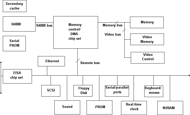
The block diagram in Figure 2.4 shows a Reduced Instruction Set Computing (RISC) system. One important difference between the designs shown in Figures 2.3 and 2.4 is the inclusion of video memory on the high speed memory bus instead of on the much slower I/O bus. This is a great benefit to graphics performance, typically improving graphical performance by a factor of between 5 and 10. This design is beginning to appear in 486-based systems as well as RISC systems.

Figure 2.4 Block diagram of a RISC-based personal computer
The main difference between Figure 2.5 and its predecessors is the addition of multiple processors. This permits multiple programs (or parts of programs, called threads) to execute simultaneously. Because they are all using the same memory, cache design is very important to reduce memory traffic and the potential for memory to be a bottleneck in such systems. The common memory usually will limit the amount of useful concurrence (ability of the multiple processors to work together) such a design will yield in practice, and the limits are very application-dependent. Although it may be difficult to predict the common memory-imposed limit, you will at least be able to determine how effective adding a new processor is once you've done it, so don't stop reading yet.

Figure 2.5 Block diagram of a multiprocessor computer